|
Contact Us
+91-11-61811100Contact Us
+91-11-61811100


We offer comprehensive system design services that cover the entire lifecycle of hardware development—from early concept and requirements gathering to PCB design, integration, testing, and validation. Our approach ensures high performance, manufacturability, and compliance in every project.
Increased electronic system design complexity coupled with time to market pressures has resulted in challenging the system designer to be innovative and adaptive to state of art technologies. Computer Aided Engineering in all stages of the design process to realize a robust and functional design. Whether it is circuit design or mechanical design or interconnects design, simulation has become the order of the day in design realization. Current day electronic systems will have to meet industry compliance standards like FCC, CISPAR, EMC, FDA. This makes it mandatory to adopt a disciplined process approach to analysis, modelling, verification, and quality process at all stages of the design.
Requirements Definition & System Architecture is the critical first step in ensuring your hardware system meets its intended purpose. We work closely with stakeholders to understand functional needs, use-case scenarios, and operational environments. From there, we define system-level specifications and outline a clear hardware architecture that maps out key components, interfaces, and power flows. This strategic planning phase ensures that the final product is not only technically sound but also aligned with performance, cost, and scalability goals—reducing development risks and accelerating time to market.
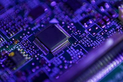
Design of the complex interconnects - “PCB Engineering” mandates that interconnect must meet the high switching rise/fall times of current day processors, memories and interface devices. This requires identifying high-speed design problems during the early stages of design by using CAE tools and in depth expertise to fix the same. This includes modelling and analysis of the connection topologies for performance in Gigabit domains.

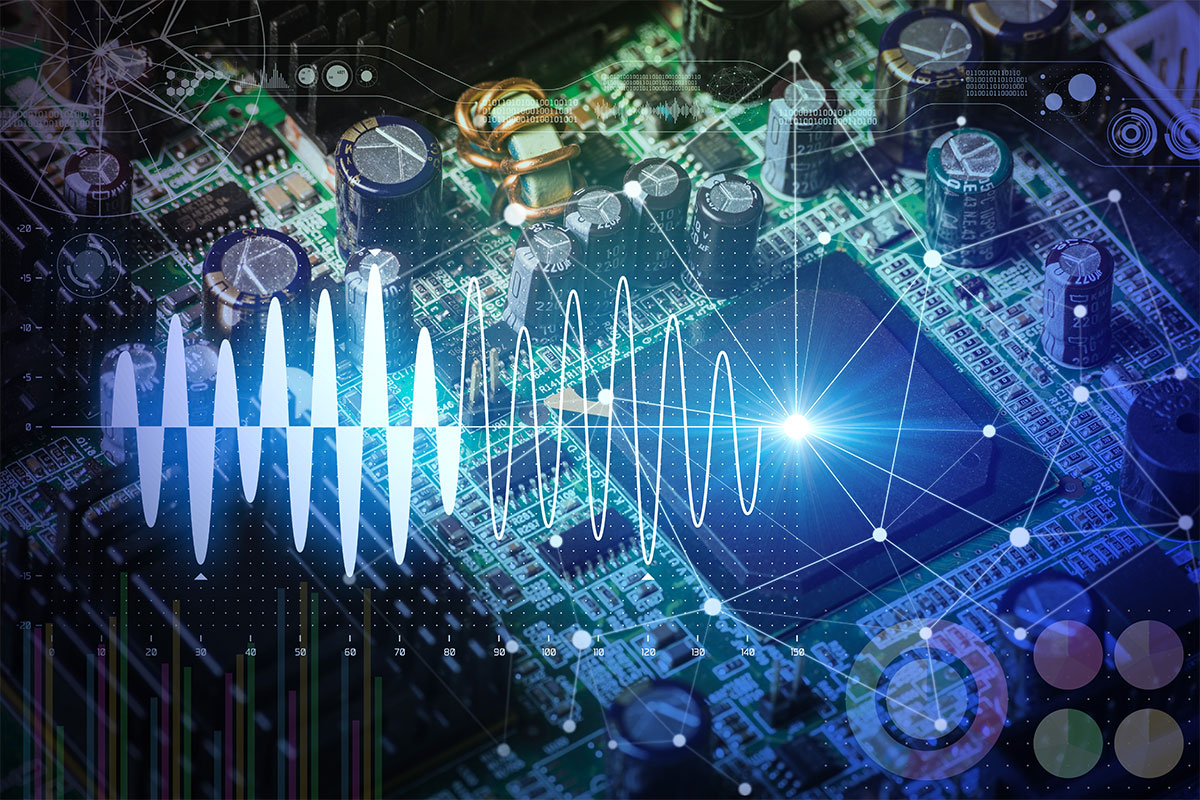
Ensuring delivery of valid signal at the receiver end in high speed designs is becoming a challenging task for a designer. This aspect of the impact of the interconnections on performance is overlooked many a time. Our team with its experience in providing solutions in analyzing designs working at Gbps is a key differentiator when ensuring a functional design in current day design technologies that use differential signalling and DDRx modules. The team can proactively address pre-layout and post layout validation of the design and validate for reflections, topologies, crosstalk and EMC to industry standards.
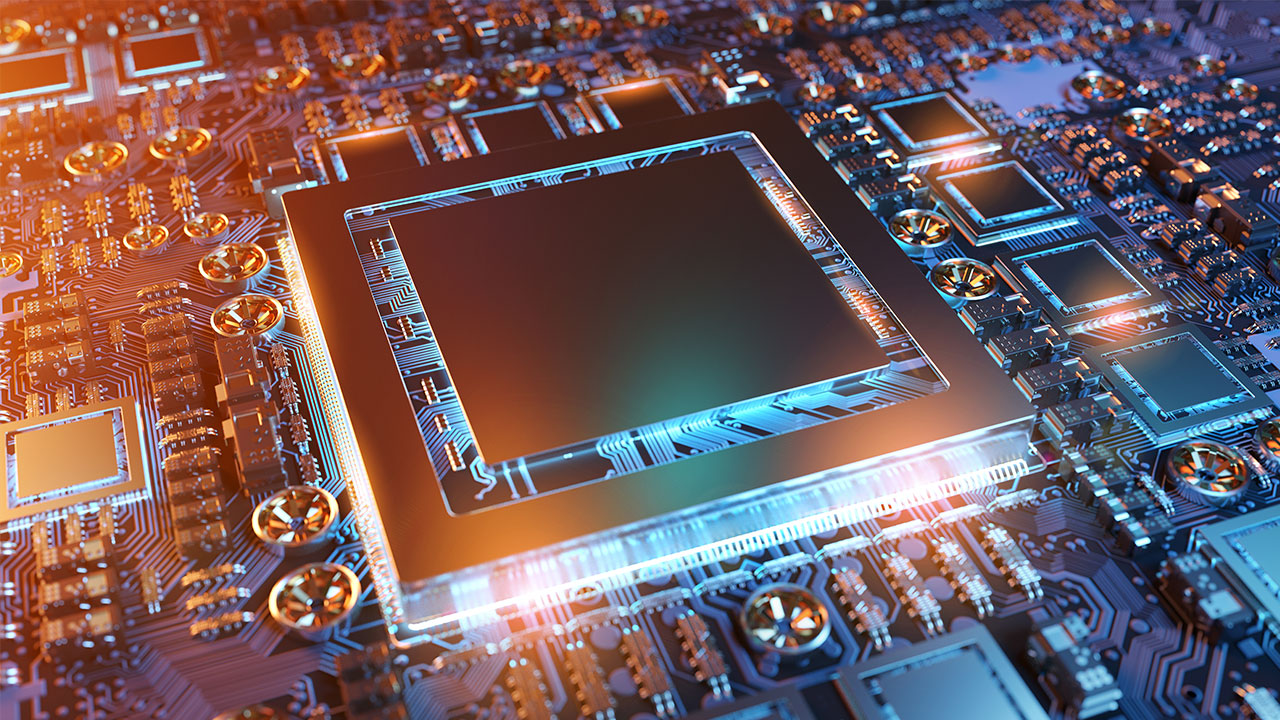
Delivering clean power to the high performance chips on a PCB is becoming a daunting task in the wake of low voltage operations of such devices. Clean power from VRM to the chip power pins meeting the DC and AC level performance demands is to be ascertained during the initial stages of design. Our team can undertake to perform power integrity analysis to ensure proper power plane design, distribution of decoupling capacitors and validating the number of decoupling capacitors to meet the AC current delivery at the operating frequency.

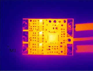
The increasing drive to integrate more functionality into compact electronic devices has led to significantly higher power densities and, consequently, greater power dissipation. This escalation directly impacts the thermal behaviour of both the PCB and the overall system, making thermal integrity a critical factor in ensuring performance, reliability, and product longevity.
Our team brings extensive expertise in board-level thermal simulation and Computational Fluid Dynamics (CFD) modelling. By leveraging industry-standard tools and advanced CFD platforms, we accurately predict thermal profiles, identify hotspots, and optimize cooling strategies. This enables us to support the development of thermally robust and functionally reliable designs, even in the most demanding operational environments.
We provide:
With our proactive approach, we ensure that your system not only meets performance expectations but does so safely and efficiently across its entire operational lifecycle.