|
Contact Us
+91-11-61811100Contact Us
+91-11-61811100

We offer end-to-end semiconductor design services - also known as semicon engineering-including ASIC design, FPGA design, and SoC design-from initial concept and specification to layout and final product realization. Our team has extensive experience in semiconductor engineering and in designing both digital and analog integrated circuits, ensuring high performance, reliability, and scalability for every application.
ASIC Design: We provide advanced ASIC design services, creating custom application-specific integrated circuits optimized for low power consumption and high-speed performance in demanding environments.
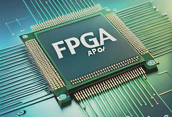
FPGA Design: Our FPGA design team develops flexible, reprogrammable hardware solutions using leading FPGA technology to meet your requirements and accelerate time-to-market.
Mixed-Signal Design: We offer comprehensive mixed-signal design, expertly integrating analog and digital circuits for robust, scalable solutions.
SoC Design: Our SoC design services cover planning and modelling of systems on a chip, including architecture, IP integration, static analysis, linting, and hardware emulation for maximum efficiency and performance.
RTL Verification: Our team performs comprehensive RTL verification (Register Transfer Level) to ensure that your digital logic behaves exactly as intended, following industry-standard best practices.
Formal Verification: We use mathematical proof techniques for formal verification, reducing risk and ensuring the highest design correctness.
Static Timing Analysis (STA): Our engineers conduct in-depth static timing analysis (STA) so that all critical paths in your design meet performance and timing constraints—supporting robust and reliable silicon.


DFT (Design for Testability): We provide DFT in VLSI to create circuits with integrated test features, improving test coverage and enabling efficient fault detection.
Post-Silicon Validation: We perform thorough post silicon validation after fabrication, ensuring your chip operates reliably and meets all functional and timing requirements in real-world conditions.
Automated Test Equipment (ATE) Support: Our experts support integration with automated test equipment (ATE) to streamline and scale semiconductor testing workflows.
Our physical design team delivers expert semiconductor engineering for floor planning, placement, routing, and timing closure—ensuring your design meets all power, performance, and area (PPA) goals.
Chip Floorplanning: We define optimal chip layouts, balancing both physical constraints and target functionality.
Placement & Routing: Our engineers optimize the placement of components and routing of connections to minimize area, reduce power usage, and ensure top performance.
Timing Analysis & Signoff: We perform advanced static timing analysis and signoff to ensure your design meets timing requirements before tape-out.

What is ASIC design
ASIC design refers to the creation of application-specific integrated circuits, which are custom chips optimized for dedicated functions, delivering high performance and low power consumption.
What services are included in FPGA design?
FPGA design services at Techlabs Semiconductor include architecture development, RTL design, simulation, synthesis, prototyping, and validation for flexible, reprogrammable hardware.
What is static timing analysis?
Static timing analysis (STA) is a method to evaluate the timing performance of a circuit without requiring simulation, ensuring all critical paths meet required timing constraints.
Do you provide post-silicon validation?
Yes, Techlabs Semiconductor performs comprehensive post-silicon validation to ensure chips function correctly in real-world conditions after fabrication.